About CDS
We develop Design and Layout software created by Designers and Engineers. We built this software platform out of necessity in our own design bureau back in 1995. We have built custom software programs in partnership with leading manufactures time and time again. With their input and use, we offer design tools that fit the need of the wish list for designers challenged in the industry to produce.
Authorized Autodesk Developer
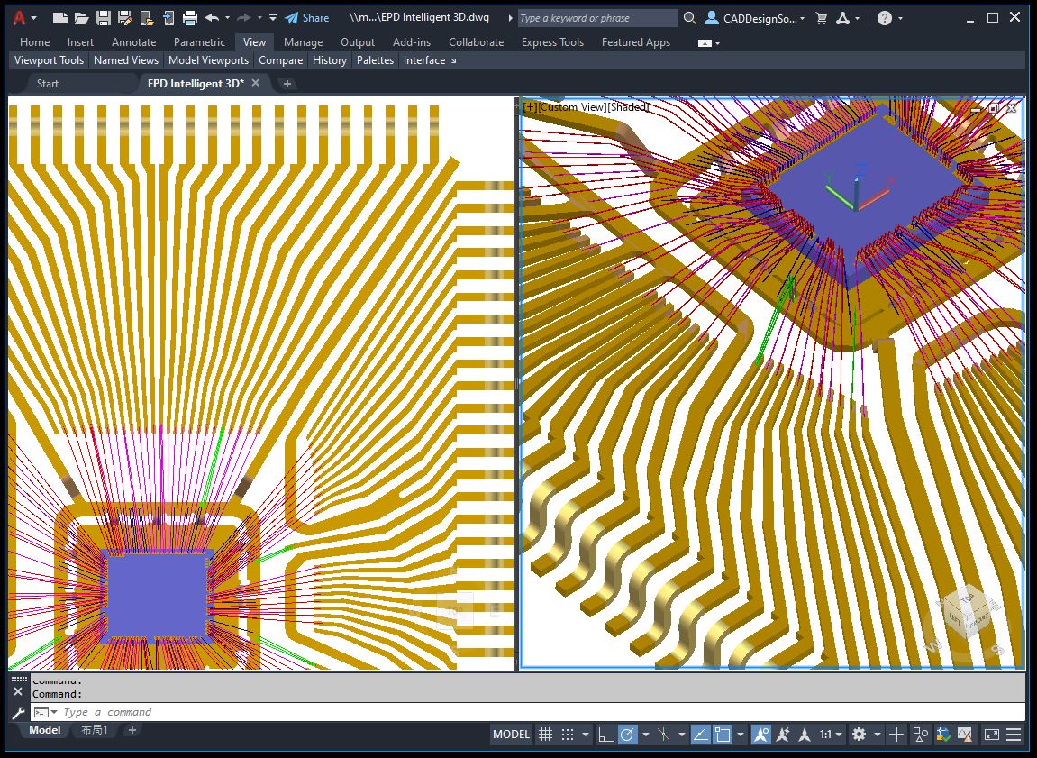
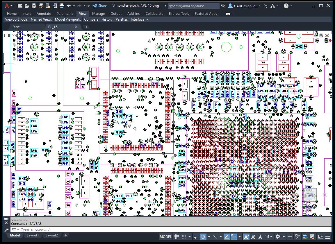
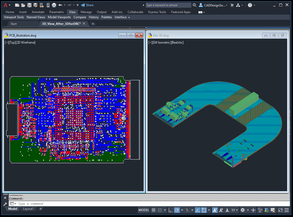
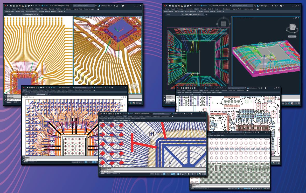
CDS has been creating software for 25+ years using the AutoCAD® engine as a base graphics engine. Using LISP and ARX routines we call this intelligent design engine, Electronics Packaging Designer or EPD. This core design engine (EPD) is tailored for specific technologies and industries. The result is faster, more accurate designs than are possible with other "Design Automation" tools. Electronics Packaging Designer (EPD) is the best environment for all types of designs and layouts.
Your Major Investment
We also realize that you have a major investment in your processes and your tools. We look at how we can improve and optimize your process and system, not throw out what you have. We reduce design time by adding automation to your processes, at a lower cost of entry than traditional EDA tools. This helps you increase productivity and also improve cost avoidance. We not only offer full stand-alone EDA layout tools, but we also complement the tools you already have through system interoperability.
Used by well-known industries in the world
EDA Software Partnerships

CAD Design Software, we believe that partnerships with leading technology companies will better the design world to help produce the best and most accurate designs with improved Return On Investment (ROI). CAD Design Software has built relationships with other EDA and software companies to expand our product line to be used on many different platforms.
Why Choose Us
Testimonials
The special LTCC design and Gerber package that CDS has designed for LTCC has essentially allowed us to reduce our tooling generation time for complex ceramic designs from 40-80 hrs to 2-8 hrs. This is a significant savings in cost, production flow and quality of our LTCC products.
I have found this to be a very good tool indeed, and I am very impressed by the features and stability. Clearly it has been designed with RF/hybrid and package design in mind, which is a huge improvement on attempting to do these designs in a PCB tool
One of our main targets is speeding up HDS (High-Density Substrate) designs. Our tests show that your system was the most powerful. You can beat most CAD or CAM systems in speed. I highly appreciate your great efforts to cause these excellent results.
CAD Design Software listed by The Silicon Review as one of the 30 Smartest Companies of the Year 2024
“Our core philosophy is rooted in the understanding that we, as designers, know what is needed out there. We’re not just creating another software program; we’re creating a tool that we, as designers, wanted and needed”
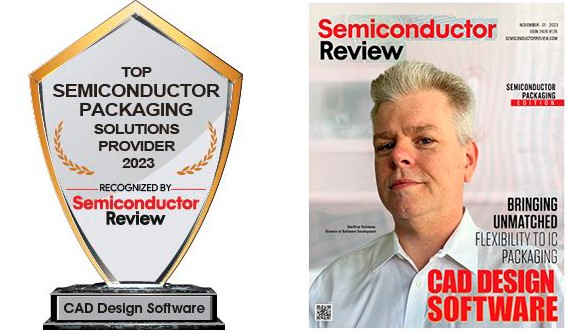
CAD Design Software is awarded in the Top 10 Semiconductor Packaging Solutions Companies of 2023 – With the advancing functionalities of integrated circuits (IC), there has been an industry-wide push toward more efficient packaging to optimize their performance. Semiconductor manufacturers look for innovative electronic design automation (EDA) software with the flexibility to simulate various design scenarios and test the manufacturability of complex IC packaging structures.
"Top 10 Developments" in Ceramic Interconnect Technology Announced at IMAPS Washington, DC – The latest advances and challenges – “The Top Ten Developments in Ceramic Interconnect Technology” – were recognized at a recent press event hosted by the Ceramic Interconnect Initiative (CII) at IMAPS 2002, The 35th International Symposium on Microelectronics in Denver, Colorado. CAD-Design Software's "Hybrid Designer” has been nominated for the honor of being included in the Ceramic Interconnect Initiative's "Top 10 Ceramic Accomplishments for 2002".
CDS RECEIVES PRESTIGIOUS AWARD FROM ADVANCED PACKAGING MAGAZINE, which each year awards the semiconductor packaging industry’s most innovative companies with a prestigious recognition of excellence for electronic packaging applications. CAD Design Software's Bond Wire Optimizer/3D Design won in the CAD Package Design Software & Equipment category
A Spectrum of EDA Functionality is Essential for PCB Design Workflows, Designing PCBs doesn’t have to be difficult if you have a comprehensive array of EDA functionality. Think of it as choosing the right tool for the right job.


